
1. Getting Started
2. Verilog Language
3. Circuits
4. Verification: Reading Simulations
5. Verification: Writing Testbenches
6. CS450
2 Verilog Language
2.1 Basics
wire
- Create a module with one input and ont output that behaves like a wire
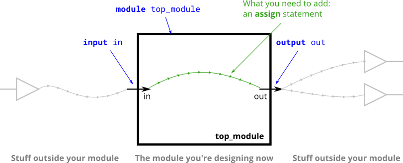
module top_module( input in, output out);

    assign out = in;

endmodule
multi-in-out
- Create a module with 3 inputs and 4 outputs that behaves like wires that makes these connections:
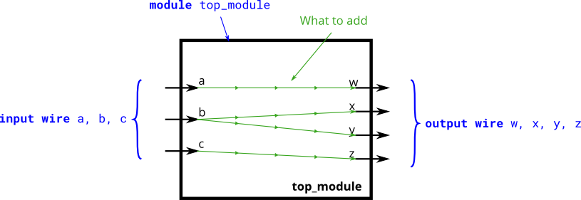
module top_module(
    input a,b,c,
    output w,x,y,z );

    assign w = a;
    assign x = b;
    assign y = b;
    assign z = c;

endmodule
not gate
- Create a module that implements a NOT gate.
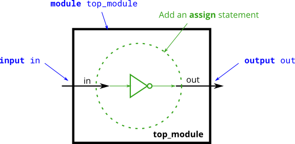
module top_module( input in, output out );

    assign out = ~in;

endmodule
and gate
- Create a module that implments an AND gate.
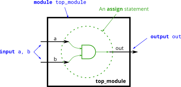
module top_module(
    input a,b,
    output out );

    assign out = a & b;

endmodule
nor gate
- Create a module that implements a NOR gate. A NOR gate is an OR gate with its output inverted. A NOR function needs two operators when written in Verilog.
module top_module(
    input a,b,
    output out );

    assign out = ~(a|b);

endmodule
xnor gate
- Create a module that implements a XNOR gate.

module top_module(
    input a, b,
    output out );

    assign out = ~(a^b);

endmodule
wire declaration
- Implement following circuits. Create two intermediate wires to connect the AND and OR gates together. Note that the wire that feeds the NOT gate is really wire out, so you do not necessarily need to declare a third wire here. Notice how wires are driven by exactly one source (output of a gate), but can feed multiple inputs.
module top_module(
    input a,b,c,d,
    output out, out_n );

    wire w1, w2;
    assign w1 = a & b;
    assign w2 = c & d;
    assign out = w1 | w2;
    assign out_n = ~out;

endmodule
7458
- The 7458 is a chip with four AND gates and two OR gates. Create a module with the same functionality as the 7458 chip. It has 10 inputs and 2 outputs.
module top_module(
    input p1a, p1b, p1c, p1d, p1e, p1f,
    output p1y,
    intput p2a, p2b, p2c, p2d,
    output p2y );

    wire w1a, w1b;
    wire w2a, w2b;

    assign w1a = p1a & p1b & p1c;
    assign w1b = p1d & p1e & p1f;
    assign p1y = w1a | w1b;
    assign w2a = p2a & p2b;
    assign w2b = p2c & p2d;
    assign p2y = w2a | w2b;

endmodule
2.2 Vectors
vector
- Build a circuit that has one 3-bit input, then outputs the same vector, and also splits it into three separate 1-bit outputs. Connect outputs o0 to the input vector’s position 0, o1 to position 1, etc.
In a diagram, a tick mark with a number next to it indicates the width of the vector (or “bus”), rather than drawing a separate line for each bit in the vector.
module top_module (
    input wire [2:0] vec,
    output wire [2:0] outv,
    output wire o2,
    output wire o1,
    output wire o0  );

    assign outv = vec;
    assign o0 = vec[0];
    assign o1 = vec[1];
    assign o2 = vec[2];

endmodule
vector select
- Build a combinational circuit that splits an input half-word (16 bits, [15:0]) into lower [7:0] and upper [15:8] bytes.
module top_module (
    input [15:0] in,
    output [7:0] out_hi,
    output [7:0] out_lo );

    assign out_hi = in[15:8];
    assign out_lo = in[7:0];

endmodule
vector swap
- A 32-bit vector can be viewed as containing 4 bytes (bits [31:24], [23:16], etc.). Build a circuit that will reverse the byte ordering of the 4-byte word.
AaaaaaaaBbbbbbbbCcccccccDddddddd => DdddddddCcccccccBbbbbbbbAaaaaaaa
This operation is often used when the endianness of a piece of data needs to be swapped, for example between little-endian x86 systems and the big-endian formats used in many Internet protocols.
module top_module (
    input [31:0] in,
    output [31:0] out
);
    assign out[31:24] = in[ 7: 0];
    assign out[23:16] = in[15: 8];
    assign out[15: 8] = in[23:16];
    assign out[ 7: 0] = in[31:24];

endmodule
vector gates
- uild a circuit that has two 3-bit inputs that computes the bitwise-OR of the two vectors, the logical-OR of the two vectors, and the inverse (NOT) of both vectors. Place the inverse of b in the upper half of out_not (i.e., bits [5:3]), and the inverse of a in the lower half.
module top_module (
    input [2:0] a,
    input [2:0] b,
    output [2:0] out_or_bitwise,
    output out_or_logical,
    output [5:0] out_not
);

    assign out_or_bitwise = a | b;
    assign out_or_logical = a || b;
    assign out_not[2:0] = ~a;
    assign out_not[5:3] = ~b;

endmodule
gate-prefix vector
- Build a combinational circuit with four inputs, in[3:0]. There are 3 outputs:
- out_and: output of a 4-input AND gate.
- out_or: output of a 4-input OR gate.
- out_xor: outout of a 4-input XOR gate.
module top_module (
    input [3:0] in,
    output out_and,
    output out_or,
    output out_xor );

    assign out_and = & in;
    assign out_or = | in;
    assign out_xor = ^ in;

endmodule
vector concatenate
- Given several input vectors, concatenate them together then split them up into several output vectors. There are six 5-bit input vectors: a, b, c, d, e, and f, for
module top_module (
    input [4:0] a, b, c, d, e, f,
    output [7:0] w, x, y, z );

    assign {w, x, y, z} = {a, b, c, d, e, f, 2'b11};

endmodule
vector reverse
- Given an 8-bit input vector [7:0], reverse its bit ordering.
module top_module(
    input [7:0] in,
    output [7:0] out
);

    assign {out[0], out[1], out[2], out[3], out[4], out[5], out[6], out[7]} = in

endmodule
module top_module(
    input [7:0] in,
    output [7:0] out
);

    always @(*) begin
        for (int i=0; i<8; i++)
            out[i] = in[8-i-1];
    end

endmodule
module top_module(
    input [7:0] in,
    output [7:0] out
);

	generate
		genvar i;
		for (i=0; i<8; i = i+1) begin: my_block_name
			assign out[i] = in[8-i-1];
		end
	endgenerate

endmodule
vector replication
- Build a circuit that sign-extends an 8-bit number to 32 bits. This requires a concatenation of 24 copies of the sign bit (i.e., replicate bit[7] 24 times) followed by the 8-bit number itself.
module top_module (
    input [7:0] in,
    output [31:0] out );

    assign out = {{24{in[7]}}, in};

endmodule
vector replication2
- Given five 1-bit signals (a, b, c, d, and e), compute all 25 pairwise one-bit comparisons in the 25-bit output vector. The output should be 1 if the two bits being compared are equal.
module top_module (
    input a, b, c, d, e,
    output [24:0] out );

    assign out = ~{{5{a}}, {5{b}}, {5{c}}, {5{d}}, {5{e}}} ^ {5{a,b,c,d,e}};

endmodule
2.3 Modules: Hierarchy
By now, you’re familiar with a module, which is a circuit that interacts with its outside through input and output ports. Larger, more complex circuits are built by composing bigger modules out of smaller modules and other pieces (such as assign statements and always blocks) connected together. This forms a hierarchy, as modules can contain instances of other modules.
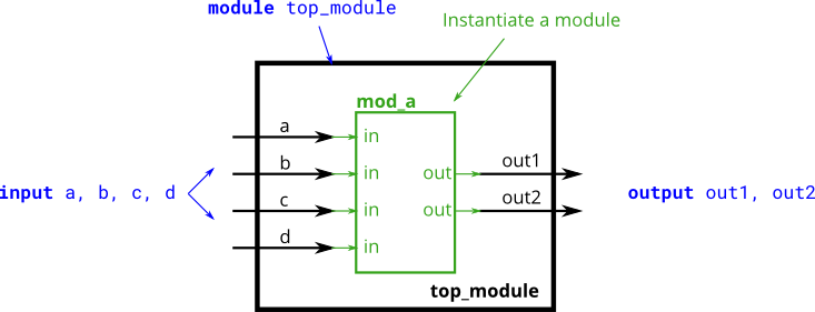
The figure below shows a very simple circuit with a sub-module. In this exercise, create one instance of module mod_a, then connect the module’s three pins (in1, in2, and out) to your top-level module’s three ports (wires a, b, and out). The module mod_a is provided for you — you must instantiate it.
When connecting modules, only the ports on the module are important. You do not need to know the code inside the module. The code for module mod_a looks like this:
module mod_a ( input in1, input in2, output out );
    // Module body
endmodule
The hierarchy of modules is created by instantiating one module inside another, as long as all of the modules used belong to the same project (so the compiler knows where to find the module). The code for one module is not written inside another module’s body (Code for different modules are not nested).
You may connect signals to the module by port name or port position. For extra practice, try both methods.
Connecting Signals to Module Ports
There are two commonly-used methods to connect a wire to a port: by position or by name.
By position
The syntax to connect wires to ports by position should be familiar, as it uses a C-like syntax. When instantiating a module, ports are connected left to right according to the module’s declaration. For example:
mod_a instance1 ( wa, wb, wc );
This instantiates a module of type mod_a and gives it an instance name of “instance1”, then connects signal wa (outside the new module) to the first port (in1) of the new module, wb to the second port (in2), and wc to the third port (out). One drawback of this syntax is that if the module’s port list changes, all instantiations of the module will also need to be found and changed to match the new module.
By name
Connecting signals to a module’s ports by name allows wires to remain correctly connected even if the port list changes. This syntax is more verbose, however.
mod_a instance2 ( .out(wc), .in1(wa), .in2(wb) );
The above line instantiates a module of type mod_a named “instance2”, then connects signal wa (outside the module) to the port named in1, wb to the port named in2, and wc to the port named out. Notice how the ordering of ports is irrelevant here because the connection will be made to the correct name, regardless of its position in the sub-module’s port list. Also notice the period immediately preceding the port name in this syntax.
module
module top_module ( input a, input b, output out );

    mod_a u_mod_a (
        .in1 (a),
        .in2 (b),
        .out (out)
    );

endmodule
module_pos
- This problem is similar to the previous one (module). You are given a module named mod_a that has 2 outputs and 4 inputs, in that order. You must connect the 6 ports by position to your top-level module’s ports out1, out2, a, b, c, and d, in that order.
You are given the following module:
module top_module (
    input a, b, c, d,
    output out1, out2 );

    mod_a u_mod_a(out1, out2, a, b, c, d);

endmodule
module_name
- This problem is similar to module. You are given a module named mod_a that has 2 outputs and 4 inputs, in some order. You must connect the 6 ports by name to your top-level module’s ports:You are given the following module:
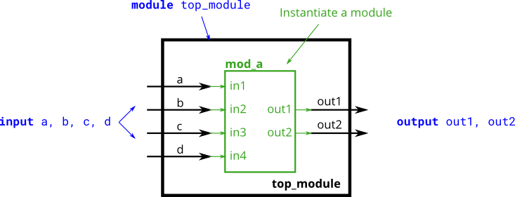
module top_module (
    input a,
    input b,
    input c,
    input d,
    output out1,
    output out2
);

    mod_a u_mod_a(
        .out1 (out1),
        .out2 (out2),
        .in1  (a),
        .in2  (b),
        .in3  (c),
        .in4  (d)
    );

endmodule
module_shift
- You are given a module my_dff with two inputs and one output (that implements a D flip-flop). Instantiate three of them, then chain them together to make a shift register of length 3. The clk port needs to be connected to all instances.
Note that to make the internal connections, you will need to declare some wires. Be careful about naming your wires and module instances: the names must be unique.
The module provided to you is:module my_dff ( input clk, input d, output q );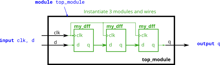
module top_module ( input clk, input d, output q );

    wire q1;
    wire q2;

    my_dff(clk, d, q1);
    my_dff(clk, q1, q2);
    my_dff(clk, q2, q);

endmodule
module_shift8
- You are given a module my_dff8 with two inputs and one output (that implements a set of 8 D flip-flops). Instantiate three of them, then chain them together to make a 8-bit wide shift register of length 3. In addition, create a 4-to-1 multiplexer (not provided) that chooses what to output depending on sel[1:0]: The value at the input d, after the first, after the second, or after the third D flip-flop. (Essentially, sel selects how many cycles to delay the input, from zero to three clock cycles.)
The module provided to you is:
module my_dff8 ( input clk, input [7:0] d, output [7:0] q );
The multiplexer is not provided. One possible way to write one is inside an always block with a case statement inside.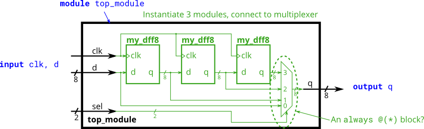
module top_module (
    input clk,
    input [7:0] d,
    input [1:0] sel,
    output [7:0] q
);
    wire [7:0] q1;
    wire [7:0] q2;
    wire [7:0] q3;
    my_dff8 (clk, d, q1);
    my_dff8 (clk, q1, q2);
    my_dff8 (clk, q2, q3);

    // multiplexer: mux9to1v
    always@(*) begin
        case(sel)
            2'd0: q = d;
            2'd1: q = q1;
            2'd2: q = q2;
            2'd3: q = q3;
        endcase
    end

endmodule
module_Half Adder
- You are given a module add16 that performs a 16-bit addition. Instantiate two of them to create a 32-bit adder. One add16 module computes the lower 16 bits of the addition result, while the second add16 module computes the upper 16 bits of the result, after receiving the carry-out from the first adder. Your 32-bit adder does not need to handle carry-in (assume 0) or carry-out (ignored), but the internal modules need to in order to function correctly. (In other words, the add16 module performs 16-bit a + b + cin, while your module performs 32-bit a + b).
Connect the modules together as shown in the diagram below. The provided module add16 has the following declaration:module add16 ( input[15:0] a, input[15:0] b, input cin, output[15:0] sum, output cout );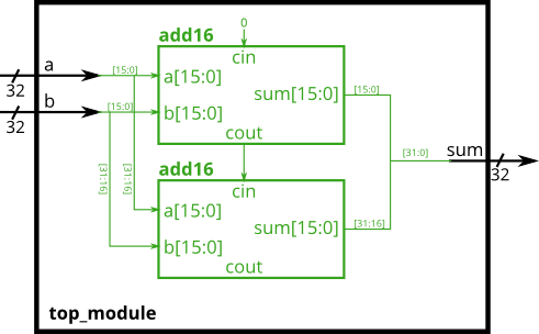
module top_module(
    input [31:0] a,
    input [31:0] b,
    output [31:0] sum
);
    wire [15:0] sum1;
    wire [15:0] sum2;
    wire cout1;
    wire cout2;

    add16 (a[15:0], b[15:0], 1'b0, sum1, cout1);
    add16 (a[31:16], b[31:16], cout1, sum2, cout2);

    assign sum = {sum2, sum1};

endmodule
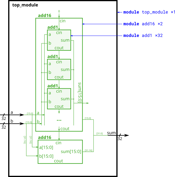
module_Full Adder
- You are given a module add16 that performs a 16-bit addition. You must instantiate two of them to create a 32-bit adder. One add16 module computes the lower 16 bits of the addition result, while the second add16 module computes the upper 16 bits of the result. Your 32-bit adder does not need to handle carry-in (assume 0) or carry-out (ignored).
Connect the add16 modules together as shown in the diagram below. The provided module add16 has the following declaration:module add16 ( input[15:0] a, input[15:0] b, input cin, output[15:0] sum, output cout );
Within each add16, 16 full adders (module add1, not provided) are instantiated to actually perform the addition. You must write the full adder module that has the following declaration:module add1 ( input a, input b, input cin, output sum, output cout );
Recall that a full adder computes the sum and carry-out of a+b+cin.
In summary, there are three modules in this design:- top_module — Your top-level module that contains two of…
- add16, provided — A 16-bit adder module that is composed of 16 of…
- add1 — A 1-bit full adder module.
module top_module (
    input [31:0] a,
    input [31:0] b,
    output [31:0] sum
);

    wire [15:0] sum1;
    wire [15:0] sum2;
    wire cout1;
    wire cout2;

    add16 (a[15:0], b[15:0], 1'b0, sum1, cout1);
    add16 (a[31:16], b[31:16], cout1, sum2, cout2);
    assign sum = {sum2, sum1};

endmodule

module add1 ( input a, input b, input cin,   output sum, output cout );
    assign sum = a ^ b ^ cin;
    assign cout = (a&b)|(b&cin)|(cin&a);
    // assign {cout, sum} = a + b + cin;
endmodule
module_Carry Select Adder
- One drawback of the ripple carry adder is that the delay for an adder to compute the carry out (from the carry-in, in the worst case) is fairly slow, and the second-stage adder cannot begin computing its carry-out until the first-stage adder has finished. This makes the adder slow. One improvement is a carry-select adder, shown below. The first-stage adder is the same as before, but we duplicate the second-stage adder, one assuming carry-in=0 and one assuming carry-in=1, then using a fast 2-to-1 multiplexer to select which result happened to be correct.
You are provided with the same module add16 as the previous exercise, which adds two 16-bit numbers with carry-in and produces a carry-out and 16-bit sum. You must instantiate three of these to build the carry-select adder, using your own 16-bit 2-to-1 multiplexer.module add16 ( input[15:0] a, input[15:0] b, input cin, output[15:0] sum, output cout );
Connect the modules together as shown in the diagram below. The provided module add16 has the following declaration: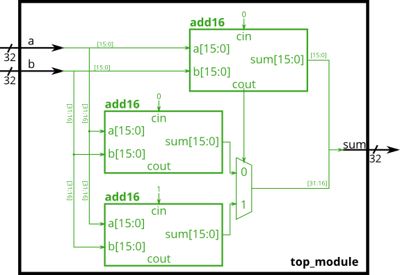
module top_module(
    input [31:0] a,
    input [31:0] b,
    output [31:0] sum
);

    wire sel;
    wire [15:0] wire0, wire1;
    add16 (a[15: 0], b[15: 0], 1'b0, sum[15:0], sel);
    add16 (a[31:16], b[31:16], 1'b0, wire0, );
    add16 (a[31:16], b[31:16], 1'b1, wire1, );

    // selector
    always@(*) begin
        case(sel)
            1'b0: sum[31:16] = wire0;
            1'b1: sum[31:16] = wire1;
        endcase
    end

    // ternary operator
    // assign sum[31:16] = sel ? wire1 : wire0;

endmodule
module_Adder-Subtractor
- An adder-subtractor can be built from an adder by optionally negating one of the inputs, which is equivalent to inverting the input then adding 1. The net result is a circuit that can do two operations: (a + b + 0) and (a + ~b + 1).
Build the adder-subtractor below.
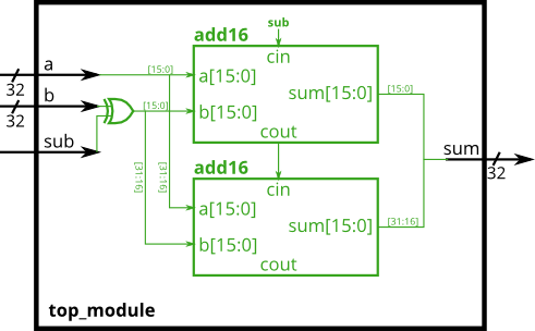 You are provided with a 16-bit adder module, which you need to instantiate twice:
module add16 ( input[15:0] a, input[15:0] b, input cin, output[15:0] sum, output cout );
Use a 32-bit wide XOR gate to invert the b input whenever sub is 1. (This can also be viewed as b[31:0] XORed with sub replicated 32 times. See replication operator.). Also connect the sub input to the carry-in of the adder.
module top_module(
    input [31:0] a,
    input [31:0] b,
    input sub,
    output [31:0] sum
);
    wire cout;
    wire [31:0] bin;

    assign bin = {32{sub}} ^ b;

    add16 (a[15: 0], bin[15: 0], sub,  sum[15: 0], cout);
    add16 (a[31:16], bin[31:16], cout, sum[31:16],     );

endmodule
2.4 Procedures
Alwaysblock
- For synthesizing hardware, two types of always blocks are relevant:
- Combinational:
always @(*) - Clocked:
always @(posedge clk)
- Combinational:
- Combinational always blocks are equivalent to assign statements, thus there is always a way to express a combinational circuit both ways. The choice between which to use is mainly an issue of which syntax is more convenient. The syntax for code inside a procedural block is different from code that is outside. Procedural blocks have a richer set of statements (e.g., if-then, case), cannot contain continuous assignments*, but also introduces many new non-intuitive ways of making errors. (*Procedural continuous assignments do exist, but are somewhat different from continuous assignments, and are not synthesizable.)
- For combinational always blocks, always use a sensitivity list of (*). Explicitly listing out the signals is error-prone (if you miss one), and is ignored for hardware synthesis. If you explicitly specify the sensitivity list and miss a signal, the synthesized hardware will still behave as though (*) was specified, but the simulation will not and not match the hardware’s behaviour. (In SystemVerilog, use always_comb.)
- A note on wire vs. reg: The left-hand-side of an assign statement must be a net type (e.g., wire), while the left-hand-side of a procedural assignment (in an always block) must be a variable type (e.g., reg). These types (wire vs. reg) have nothing to do with what hardware is synthesized, and is just syntax left over from Verilog’s use as a hardware simulation language.
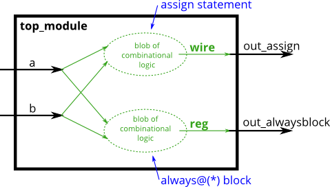
- Build an AND gate using both an assign statement and a combinational always block.
module top_module(
    input a,
    input b,
    output wire out_assign,
    output reg out_alwaysblock
);

	assign out_assign = a & b;

    always @(*) begin
    	out_alwaysblock = a & b;
    end

endmodule
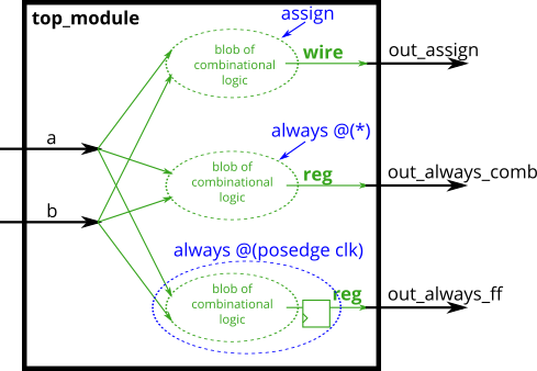
Clocked
Clocked always blocks create a blob of combinational logic just like combinational always blocks, but also creates a set of flip-flops (or “registers”) at the output of the blob of combinational logic. Instead of the outputs of the blob of logic being visible immediately, the outputs are visible only immediately after the next (posedge clk). Blocking vs. Non-Backing Assignment
There are three types of assignments in Verilog:
- Continuous assignments (
assign x = y;): Can only be used when not inside a procedure (“always block”). - Procedural blocking assignment (
x = y;): Can only be used inside a procedure. - Procedural non-blocking assignment (
x <= y;): Can only be used inside a procedure.
- Continuous assignments (
In a combinational always block, use blocking assignments. In a clocked always block, used non-blocking assignments. A full understanding of why is not particularly usedful for hardware design and requires a good understanding of how Verilog simulators keep track of events. Not following this rule results in extremely hard to find errors that are both non-deterministic and differ between simulation and synthesized hardware.
Build an XOR gate three ways, using an assignment, a combinational always block, and a clocked always block. Note that the clocked always block precedures a different circuit from the other two: There is a flip-flop so the output is delayed.
module top_module(
    input clk,
    input a,
    input b,
    output wire out_assign,
    output reg out_always_comb,
    output reg out_always_ff   );

    assign out_assign = a ^ b;
    always @(*) begin
    	out_always_comb = a ^ b;
    end
    always @(posedge clk) begin
		out_always_ff <= a ^ b;
    end

endmodule
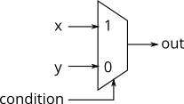
If statement
- An if statement usually creates a 2-to-1 multiplexer, selecting one input if the condition is true, and the other input if the condition is false.
always @(*) begin
    if (condition) begin
        out = x;
    end
    else begin
        out = y;
    end
end
This is equivalent to using a continuous assignment with a conditional operator:
assign out = (condition) ? x : y;However, the procedural if statement provides a new way to make mistakes. The circuit is combinational only if out is always assigned a value.
Build a 2-to-1 mux that chooses between a and b. Choose b if both sel_b1 and sel_b2 are true. Otherwise, choose a. Do the same twice, once using assign statements and once using a procedural if statement. \(\begin{array}{|c|c|c|}\hline \text{sel\_b1}&\text{sel\_b2}&\text{out\_assign, out\_always} \\\hline 0&0&a\\\hline 0&1&a\\\hline 1&0&a\\\hline 1&1&b\\\hline \end{array
module top_module(
    input a,
    input b,
    input sel_b1,
    input sel_b2,
    output wire out_assign,
    output reg out_always   );

    assign out_assign = sel_b1 & sel_b2 ? b : a;

    always @(*) begin
        if (sel_b1 & sel_b2) begin
        	out_always = b;
        end
        else begin
        	out_always = a;
        end
    end

    // always @(*) begin
    //    case ({sel_b1, sel_b2})
	//		2'd0:begin
	//			out_always = a;
    //        end
    //        2'd1:begin
	//			out_always = a;
    //        end
    //        2'd2:begin
	//			out_always = a;
    //        end
    //        2'd3:begin
	//			out_always = b;
    //        end
    //    endcase
    // end

endmodule
If statement latches
A common source of errors: How to avoid making latches
When designing circuits, you must think first in terms of circuits:
- I want this logic gate
- I want a combinational blob of logic that has these inputs and produces these outputs
- I want a combinational blob of logic followed by a set of flip-flops
What you must not do is write the code first, then hope it generates a proper circuit.
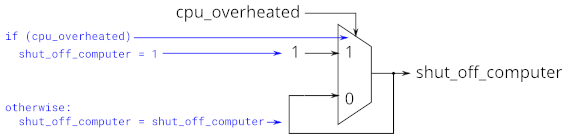
- If (cpu_overheated) then shut_off_computer = 1;
- If (~arrived) then keep_driving = ~gas_tank_empty;
Syntactically-correct code does not necessarily result in a reasonable circuit (combinational logic + flip-flops). The usual reason is: “What happens in the cases other than those you specified?”. Verilog’s answer is: Keep the outputs unchanged.
This behaviour of “keep outputs unchanged” means the current state needs to be remembered, and thus produces a latch. Combinational logic (e.g., logic gates) cannot remember any state. Watch out for Warning (10240): … inferring latch(es)" messages. Unless the latch was intentional, it almost always indicates a bug. Combinational circuits must have a value assigned to all outputs under all conditions. This usually means you always need else clauses or a default value assigned to the outputs.
Demonstration
- The following code contains incorrect behaviour that creates a latch. Fix the bugs so that you will shut off the computer only if it’s really overheated, and stop driving if you’ve arrived at your destination or you need to refuel.
always @(*) begin
    if (cpu_overheated)
        shut_off_computer = 1;
end
always @(*) begin
    if (~arrived)
        keep_driving = ~gas_tank_empty;
end
module top_module (
    input      cpu_overheated,
    output reg shut_off_computer,
    input      arrived,
    input      gas_tank_empty,
    output reg keep_driving  ); //

    always @(*) begin
        if (cpu_overheated)
            shut_off_computer = 1;
        else
            shut_off_computer = 0;
    end

    always @(*) begin
        if (~arrived)
            keep_driving = ~gas_tank_empty;
        else
            keep_driving = 0;
    end

endmodule
Case statement
- Case statements in Verilog are nearly equivalent to a sequence of if-elseif-else that compares one expression to a list of others. Its syntax and functionality differs from the switch statement in C.
always @(*) begin     // This is a combinational circuit
    case (in)
      1'b1: begin
               out = 1'b1;  // begin-end if >1 statement
            end
      1'b0: out = 1'b0;
      default: out = 1'bx;
    endcase
end
The case statement begins with case and each “case item” ends with a colon. There is no “switch”. Each case item can execute exactly one statement. This makes the “break” used in C unnecessary. But this means that if + you need more than one statement, you must use
begin ... end.Duplicate (and partially overlapping) case items are permitted. The first one that matches is used. C does not allow duplicate case items.
Create a 6-to-1 multiplexer. When sel is between 0 and 5, choose the corresponding data input. Otherwise, output 0. The data inputs and outputs are all 4 bits wide. Be careful of inferring latches.
// synthesis verilog_input_version verilog_2001
module top_module (
    input [2:0] sel,
    input [3:0] data0,
    input [3:0] data1,
    input [3:0] data2,
    input [3:0] data3,
    input [3:0] data4,
    input [3:0] data5,
    output reg [3:0] out   );

    always @(*) begin
        case(sel)
            0: out = data0;
			1: out = data1;
            2: out = data2;
            3: out = data3;
            4: out = data4;
            5: out = data5;
            default: out = 0;
        endcase
    end

endmodule
Priority encoder
- A priority encoder is a combinational circuit that, when given an input bit vector, outputs the position of the first 1 bit in the vector. For example, a 8-bit priority encoder given the input
8'b10010000would output 3’d4, because bit[4] is first bit that is high. - Build a 4-bit priority encoder. For this problem, if none of the input bits are high (i.e., input is zero), output zero. Note that a 4-bit number has 16 possible combinations.
module top_module (
	input [3:0] in,
	output reg [1:0] pos
);

	always @(*) begin
		case (in)
			4'h0: pos = 2'h0;  //0000
			4'h1: pos = 2'h0;  //0001
			4'h2: pos = 2'h1;  //0010
			4'h3: pos = 2'h0;  //0011
			4'h4: pos = 2'h2;  //0100
			4'h5: pos = 2'h0;  //0101
			4'h6: pos = 2'h1;  //0110
			4'h7: pos = 2'h0;  //0111
			4'h8: pos = 2'h3;  //1000
			4'h9: pos = 2'h0;  //1001
			4'ha: pos = 2'h1;  //1010
			4'hb: pos = 2'h0;  //1011
			4'hc: pos = 2'h2;  //1100
			4'hd: pos = 2'h0;  //1101
			4'he: pos = 2'h1;  //1110
			4'hf: pos = 2'h0;  //1111
			default: pos = 2'b0;
		endcase
	end
endmodule
Priority encoder with casez
- Build previous problem with
casez. If the case items in the case statement supported con’t care bits. This is what casez is for: It treats bits that have the value z as don’t care in the comparison. - A case statement behaves as though each item is checked sequentially (in reality, a big combinational logic function). Notice how there are certain inputs (e.g., 4’b1111) that will match more than one case item. The first match is chosen (so 4’b1111 matches the first item, out = 0, but not any of the later ones).
- There is also a similar casex that treats both x and z as don’t-care. I don’t see much purpose to using it over casez.
- The digit ? is a synonym for z. so 2’bz0 is the same as 2’b?0
- It may be less error-prone to explicitly specify the priority behaviour rather than rely on the ordering of the case items. For example, the following will still behave the same way if some of the case items were reordered, because any bit pattern can only match at most one case item:
module top_module (
    input [7:0] in,
    output reg [2:0] pos  );

    always @(*) begin
        casez(in)
            8'bzzzzzzz1: pos = 3'd0;
            8'bzzzzzz10: pos = 3'd1;
            8'bzzzzz100: pos = 3'd2;
            8'bzzzz1000: pos = 3'd3;
            8'bzzz10000: pos = 3'd4;
            8'bzz100000: pos = 3'd5;
            8'bz1000000: pos = 3'd6;
            8'b10000000: pos = 3'd7;
            default: pos = 2'd0;
        endcase
    end

endmodule
Avoiding latches
- Suppose you’re building a circuit to process scancodes from a PS/2 keyboard for a game. Given the last two bytes of scancodes received, you need to indicate whether one of the arrow keys on the keyboard have been pressed. This involves a fairly simple mapping, which can be implemented as a case statement (or if-elseif) with four cases.
\(\begin{array}{|c|c|}\hline \text{Scancode [15:0]}&\text{Arrow key}\\\hline \text{16’he06b}&\text{left arrow}\\\hline \text{16’he072}&\text{down arrow}\\\hline \text{16’he074}&\text{right arrow}\\\hline \text{16’he075}&\text{up arrow}\\\hline \text{Anything else}&\text{none}\\\hline \end{array - Your circuit has one 16-bit input, and four outputs. Build this circuit that recognizes these four scancodes and asserts the correct output.
- To avoid creating latches, all outputs must be assigned a value in all possible conditions. Simply having a
defaultcase is not enough. You must assign a value to all four outputs in all four cases and the default case. This can involve a lot of unnecessary typing. One easy way around this is to assign a “default value” to the outputs before the case statement:
always @(*) begin
    up = 1'b0; down = 1'b0; left = 1'b0; right = 1'b0;
    case (scancode)
        ... // Set to 1 as necessary.
    endcase
end
- This style of code ensures the outputs are assigned a value (of 0) in all possible cases unless the case statement overrides the assignment. This also means that a default: case item becomes unnecessary.
- Reminder: The logic synthesizer generates a combinational circuit that behaves equivalently to what the code describes.Hardware does not “execute” the lines of code in sequence.
module top_module (
    input [15:0] scancode,
    output reg left,
    output reg down,
    output reg right,
    output reg up  );

    always @(*) begin
        left = 0;
        down = 0;
        right = 0;
        up = 0;
        case(scancode)
			16'he06b: left = 1;
			16'he072: down = 1;
			16'he074: right = 1;
			16'he075: up = 1;
        endcase
    end
endmodule
2.5 More Verilog Features
Conditional ternary operator
- Verilog has a ternary conditional operator ( ? : ) much like C:
(condition ? if_true : if_false) - Given four unsigned numbers, find the minimum. Unsigned numbers can be compared with standard comparison operators (a < b). Use the conditional operator to make two-way min circuits, then compose a few of them to create a 4-way min circuit. You’ll probably want some wire vectors for the intermediate results.
module top_module (
    input [7:0] a, b, c, d,
    output [7:0] min);//

    wire [7:0] wire1;
    wire [7:0] wire2;

    assign wire1 = a > b ? b : a;
    assign wire2 = c > d ? d : c;
    assign min = wire1 > wire2 ? wire2 : wire1;

endmodule
Reduction operators
- Some syntactic sugar for reduction:
& a[3:0]    // AND: a[3] & a[2] & a[1] & a[0]. Equivalent to (a[3:0] == 4'hf)
| b[3:0]    // OR: b[3] | b[2] | b[1] | b[0]. Equivalent to (b[3:0] != 4'h0)
^ c[2:0]    // XOR: c[2] ^ c[1] ^ c[0]
- Parity checking is often used as a simple method of detecting errors when transmitting data through an imperfect channel. Create a circuit that will compute a parity bit for a 8-bit byte (which will add a 9th bit to the byte). We will use “even” parity, where the parity bit is just the XOR of all 8 data bits.
module top_module (
    input [7:0] in,
    output parity);

    assign parity = ^ in;

endmodule
Reduction: Even wider gates
- Build a combinational circuit with 100 inputs, in[99:0]. There are 3 outputs:
- out_and: output of a 100-input AND gate.
- out_or: output of a 100-input OR gate.
- out_xor: output of a 100-input XOR gate.
module top_module(
    input [99:0] in,
    output out_and,
    output out_or,
    output out_xor );

    assign out_and = & in;
    assign out_or = | in;
    assign out_xor = ^ in;

endmodule
Combinational for-loop: Vector reversal
- Given a 100-bit input vector [99:0], reverse its bit ordering.
module top_module(
    input [99:0] in,
    output [99:0] out
);

    always @(*) begin
        for (int i = 0; i < 100; i++) begin
            out[i] = in[99 - i];
        end
    end

endmodule
Combinational for-loop: 255-bit population count
- A “population count” circuit counts the number of ‘1’s in an input vector. Build a population count circuit for a 255-bit input vector.
module top_module(
    input [254:0] in,
    output [7:0] out );

    always @(*) begin
        out = 0;
        for (int i = 0; i < 255; i++) begin
            out += in[i];
        end
    end

endmodule
Generate for-loop: 100-bit binary adder
- Create a 100-bit binary ripple-carry adder by instantiating 100 full adders. The adder adds two 100-bit numbers and a carry-in to produce a 100-bit sum and carry out. To encourage you to actually instantiate full adders, also output the carry-out from each full adder in the ripple-carry adder. cout[99] is the final carry-out from the last full adder, and is the carry-out you usually see.
module top_module(
    input [99:0] a, b,
    input cin,
    output [99:0] cout,
    output [99:0] sum );

    always @(*) begin
        {cout[0], sum[0]} = a[0] + b[0] + cin;
        for (int i = 1; i < 100; i++) begin
            {cout[i], sum[i]} = a[i] + b[i] + cout[i-1];
        end
    end

endmodule
Generate for-loop: 100-digit BCD adder
- You are provided with a BCD one-digit adder named bcd_fadd that adds two BCD digits and carry-in, and produces a sum and carry-out.
module bcd_fadd (
    input [3:0] a,
    input [3:0] b,
    input     cin,
    output   cout,
    output [3:0] sum );
- Instantiate 100 copies of bcd_fadd to create a 100-digit BCD ripple-carry adder. Your adder should add two 100-digit BCD numbers (packed into 400-bit vectors) and a carry-in to produce a 100-digit sum and carry out.
module top_module(
    input [399:0] a, b,
    input cin,
    output cout,
    output [399:0] sum );

    wire[99:0] carryin;

    generate
        genvar i;
        bcd_fadd(a[3:0], b[3:0], cin, carryin[0], sum[3:0]);
        for (i = 4; i < 400; i += 4) begin:adder
            bcd_fadd(a[i+3:i], b[i+3:i], carryin[i/4-1], carryin[i/4], sum[i+3:i]);
        end
        assign cout = carryin[99];
    endgenerate
endmodule