
1. Getting Started
2. Verilog Language
3. Circuits
4. Verification: Reading Simulations
5. Verification: Writing Testbenches
6. CS450
3 Circuits
3.1 Combinational Logic
3.1.1 Basic Gates
Wire

module top_module (
    input in,
    output out);

    assign out = in;

endmodule
GND

module top_module (
    output out);

    assign out = 1'b0;

endmodule
NOR

module top_module (
    input in1,
    input in2,
    output out);

    assign out = ~(in1|in2);

endmodule
Another Gate
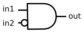
module top_module (
    input in1,
    input in2,
    output out);

    assign out = in1 & (~in2);

endmodule
Two gates

module top_module (
    input in1,
    input in2,
    input in3,
    output out);

    wire w1;

    assign w1 = ~(in1^in2);
    assign out = w1^in3;

endmodule
More logic gates
module top_module(
    input a, b,
    output out_and,
    output out_or,
    output out_xor,
    output out_nand,
    output out_nor,
    output out_xnor,
    output out_anotb
);

    assign out_and = a & b;
    assign out_or = a | b;
    assign out_xor = a ^ b;
    assign out_nand = ~(a & b);
    assign out_nor = ~(a | b);
    assign out_xnor = ~(a ^ b);
    assign out_anotb = a & (~b);

//    and(out_and, a, b);
//    or(out_or, a, b);
//    xor(out_xor, a, b);
//    nand(out_nand, a, b);
//    nor(out_nor, a, b);
//    xnor(out_xnor, a, b);
//    and(out_anotb, a , ~b);

endmodule
7420 chip
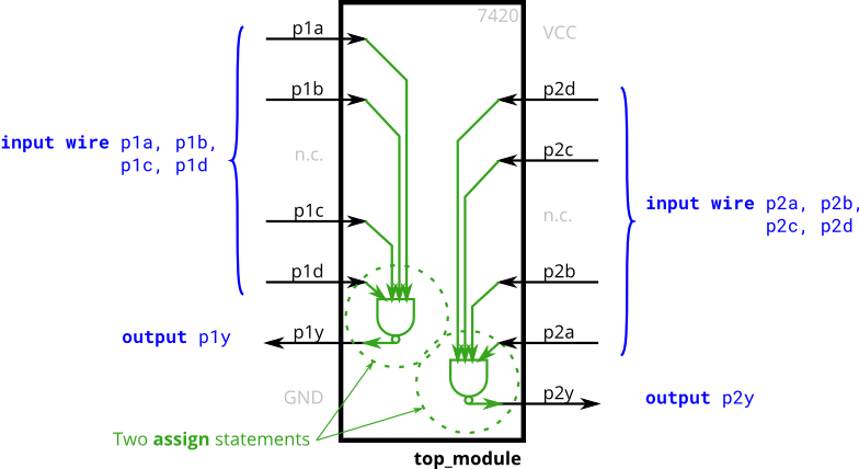
module top_module (
    input p1a, p1b, p1c, p1d,
    output p1y,
    input p2a, p2b, p2c, p2d,
    output p2y );

    assign p1y = ~(p1a & p1b & p1c & p1d);
    assign p2y = ~(p2a & p2b & p2c & p2d);

endmodule\
Truth tables
\(\begin{array}{|c|ccc|c|}\hline
\text{Row}&&\text{Inputs}&&\text{Outputs}\\\hline
\text{number}&\text{x3}&\text{x2}&\text{x1}&\text{f}\\\hline
0&0&0&0&0\\\hline
1&0&0&1&0\\\hline
2&0&1&0&1\\\hline
3&0&1&1&1\\\hline
4&1&0&0&0\\\hline
5&1&0&1&1\\\hline
6&1&1&0&0\\\hline
7&1&1&1&1\\\hline
\end{array
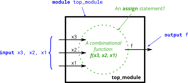
module top_module(
    input x3,
    input x2,
    input x1,
    output f );

    assign f = ((~x3)&x2)|(x3&x1);

endmodule
Two-bit equality
- Create a circuit that has two 2-bit inputs A[1:0] and B[1:0], and produces an output z. The value of z should be 1 if A = B, otherwise z should be 0.
module top_module ( input [1:0] A, input [1:0] B, output z );

    assign z = (A == B);

endmodule
Simple circuit A
module top_module (input x, input y, output z);

    assign z = (x^y) &x;

endmodule
Simple circuit B
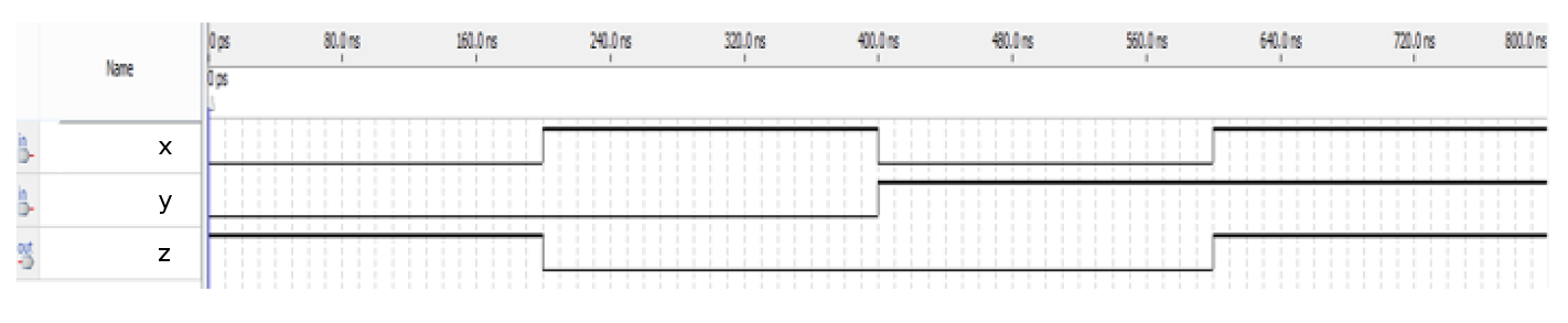
module top_module ( input x, input y, output z );

    assign z = (x==y);
    // assign z = ~(x ^ y);

endmodule
Combine circuits A and B
module top_module (input x, input y, output z);

    wire o1, o2, o3, o4;

    A ia1(x,y,o1);
    B ib1(x,y,o2);
    A ia2(x,y,o3);
    B ib2(x,y,o4);

    assign z = (o1|o2)^(o3&o4);

endmodule

module A(
    input x, y,
    output z);

    assign z = (x ^ y) & x;

endmodule

module B(
    input x, y,
    output z);

    assign z = x ~^ y;

endmodule
Ringer
- Suppose you are designing a circuit to control a cellphone’s ringer and vibration motor. Whenever the phone needs to ring from an incoming call (
input ring), your circuit must either turn on the ringer (output ringer = 1) or the motor (output motor = 1), but not both. If the phone is in vibrate mode (input vibrate_mode = 1), turn on the motor. Otherwise, turn on the ringer. - Try to use only assign statements, to see whether you can translate a problem description into a collection of logic gates.
- Design hint: When designing circuits, one often has to think of the problem “backwards”, starting from the outputs then working backwards towards the inputs. This is often the opposite of how one would think about a (sequential, imperative) programming problem, where one would look at the inputs first then decide on an action (or output). For sequential programs, one would often think “If (inputs are ___ ) then (output should be ___ )”. On the other hand, hardware designers often think “The (output should be ___ ) when (inputs are ___ )”.
- The above problem description is written in an imperative form suitable for software programming (if ring then do this), so you must convert it to a more declarative form suitable for hardware implementation (
assign ringer = ___). Being able to think in, and translate between, both styles is one of the most important skills needed for hardware design.
module top_module (
    input ring,
    input vibrate_mode,
    output ringer,       // Make sound
    output motor         // Vibrate
);

    assign ringer = ring & (~vibrate_mode);
    assign motor = ring & (vibrate_mode);

endmodule
Thermostat
- A heating/cooling thermostat controls both a heater (during winter) and an air conditioner (during summer). Implement a circuit that will turn on and off the heater, air conditioning, and blower fan as appropriate.
- The thermostat can be in one of two modes: heating (
mode = 1) and cooling (mode = 0). In heating mode, turn the heater on when it is too cold (too_cold = 1) but do not use the air conditioner. In cooling mode, turn the air conditioner on when it is too hot (too_hot = 1), but do not turn on the heater. When the heater or air conditioner are on, also turn on the fan to circulate the air. In addition, the user can also request the fan to turn on (fan_on = 1), even if the heater and air conditioner are off. - Try to use only assign statements, to see whether you can translate a problem description into a collection of logic gates.
- 畫出真值表
\(\begin{array}{|cccc|ccc|}\hline \text{mode}&\text{too\_cold}&\text{too\_hot}&\text{fan on}&\text{heater}&\text{aircon}&\text{fan}\\\hline 0&0&0&0&0&0&0\\\hline 0&0&0&1&0&0&1\\\hline 0&0&1&0&0&1&1\\\hline 0&0&1&1&0&1&1\\\hline 0&1&0&0&0&0&0\\\hline 0&1&0&1&0&0&1\\\hline 0&1&1&0&0&1&1\\\hline 0&1&1&1&0&1&1\\\hline 1&0&0&0&0&0&0\\\hline 1&0&0&1&0&0&1\\\hline 1&0&1&0&0&0&0\\\hline 1&0&1&1&0&0&1\\\hline 1&1&0&0&1&0&1\\\hline 1&1&0&1&1&0&1\\\hline 1&1&1&0&1&0&1\\\hline 1&1&1&1&1&0&1\\\hline \end{array}\)
module top_module (
    input too_cold,
    input too_hot,
    input mode,
    input fan_on,
    output heater,
    output aircon,
    output fan);

    assign heater = mode & too_cold;
    assign aircon = (~mode) & too_hot;
    assign fan = heater|aircon|fan_on;

endmodule
3-bit population count
- A “population count” circuit counts the number of ‘1’s in an input vector. Build a population count circuit for a 3-bit input vector.
module top_module(
    input [2:0] in,
    output [1:0] out );

    always @(*) begin
        out = 0;
        for (int i = 0; i <= 2; i++) begin
            out += in[i];
        end
    end

endmodule
- 此解會產生鎖存器,不建議使用。
Gates and vectors
- You are given a four-bit input vector in[3:0]. We want to know some relationships between each bit and its neighbour:
- out_both: Each bit of this output vector should indicate whether both the corresponding input bit and its neighbour to the left (higher index) are ‘1’. For example,
out_both[2]should indicate ifin[2]andin[3]are both 1. Sincein[3]has no neighbour to the left, the answer is obvious so we don’t need to knowout_both[3]. - out_any: Each bit of this output vector should indicate whether any of the corresponding input bit and its neighbour to the right are ‘1’. For example,
out_any[2]should indicate if eitherin[2]orin[1]are 1. Sincein[0]has no neighbour to the right, the answer is obvious so we don’t need to knowout_any[0]. - out_different: Each bit of this output vector should indicate whether the corresponding input bit is different from its neighbour to the left. For example,
out_different[2]should indicate ifin[2]is different fromin[3]. For this part, treat the vector as wrapping around, soin[3]’s neighbour to the left isin[0].
- out_both: Each bit of this output vector should indicate whether both the corresponding input bit and its neighbour to the left (higher index) are ‘1’. For example,
module top_module(
    input [3:0] in,
    output [2:0] out_both,
    output [3:1] out_any,
    output [3:0] out_different );

    assign out_both[2:0] = in[2:0] & in[3:1];
    assign out_any[3:1] = in[3:1] | in[2:0];
    assign out_different[3:0] = in[3:0] ^ {in[0], in[3:1]};

    // always @(*) begin
    //    out_different[3] = (in[3] != in[0]);
    //    for (int i = 0; i <= 2; i++) begin
    //        out_both[i] = in[i] & in[i+1];
    //        out_any[i+1] = in[i+1] | in[i];
    //        out_different[i] = (in[i] != in[i+1]);
    //    end
    // end

endmodule
Even longer vectors
- You are given a 100-bit input vector in[99:0]. We want to know some relationships between each bit and its neighbour:
- out_both: Each bit of this output vector should indicate whether both the corresponding input bit and its neighbour to the left are ‘1’. For example,
out_both[98]should indicate ifin[98]andin[99]are both 1. Sincein[99]has no neighbour to the left, the answer is obvious so we don’t need to knowout_both[99]. - out_any: Each bit of this output vector should indicate whether any of the corresponding input bit and its neighbour to the right are ‘1’. For example,
out_any[2]should indicate if eitherin[2]orin[1]are 1. Sincein[0]has no neighbour to the right, the answer is obvious so we don’t need to knowout_any[0]. - out_different: Each bit of this output vector should indicate whether the corresponding input bit is different from its neighbour to the left. For example,
out_different[98]should indicate ifin[98]is different fromin[99]. For this part, treat the vector as wrapping around, soin[99]’s neighbour to the left isin[0].
- out_both: Each bit of this output vector should indicate whether both the corresponding input bit and its neighbour to the left are ‘1’. For example,
module top_module(
    input [99:0] in,
    output [98:0] out_both,
    output [99:1] out_any,
    output [99:0] out_different );

    assign out_both[98:0] = in[98:0] & in[99:1];
    assign out_any[99:1] = in[99:1] | in[98:0];
    assign out_different[99:0] = in[99:0] ^ {in[0], in[99:1]};

endmodule
3.1.2 Multiplexers
2-to-1 multiplexer
- Create a one-bit wide, 2-to-1 multiplexer. When sel=0, choose a. When sel=1, choose b.
module top_module(
    input a, b, sel,
    output out );

    assign out = sel ? b : a;

endmodule
2-to-1 bus multiplexer
- Create a 100-bit wide, 2-to-1 multiplexer. When sel=0, choose a. When sel=1, choose b.
module top_module(
    input [99:0] a, b,
    input sel,
    output [99:0] out );

    assign out = sel ? b : a;

endmodule
9-to-1 multiplexer
- Create a 16-bit 9-to-1 multiplexer. sel=0 chooses a, sel=1 chooses b, etc. For the unused cases (sel=9 to 15), set all output bits to ‘1’.
module top_module(
    input [15:0] a, b, c, d, e, f, g, h, i,
    input [3:0] sel,
    output [15:0] out );

    always @(*) begin
        case(sel)
            4'd0: out = a;
            4'd1: out = b;
            4'd2: out = c;
            4'd3: out = d;
            4'd4: out = e;
            4'd5: out = f;
            4'd6: out = g;
            4'd7: out = h;
            4'd8: out = i;
            default: out = '1;  // special literal syntax with all bits set to 1
        endcase
    end

endmodule
256-to-1 multiplexer
- Create a 1-bit wide, 256-to-1 multiplexer. The 256 inputs are all packed into a single 256-bit input vector. sel=0 should be select
in[0], sel1 selectes bitsin[1], sel=2 selects bitsin[2], etc.
module top_module(
    input [255:0] in,
    input [7:0] sel,
    output out );

    assign out = in[sel];

endmodule
256-to-1 4-bit multiplexer
- Create a 4-bit wide, 256-to-1 multiplexer. The 256 4-bit inputs are all packed into a single 1024-bit input vector. sel=0 should select bits
in[3:0],sel=1 selects bitsin[7:4], sel=2 selects bitsin[11:8], etc.
module top_module(
    input [1023:0] in,
    input [7:0] sel,
    output [3:0] out );

    assign out = in[sel*4+:4];  // special syntax
    // assign out = in[sel*4+3-:4];
    // assign out = {in[sel*4+3],in[sel*4+2],in[sel*4+1],in[sel*4+0]};

endmodule
3.1.3 Arithmetic Circuits
Half adder
- Create a half adder. A half adder adds two bits (with no carry-in) and produces a sum and carry-out.
module top_module(
    input a, b,
    output cout, sum );

    assign {cout, sum} = a + b;

endmodule
Full adder
- Create a full adder. A full adder adds three bits (including carry-in) and produces a sum and a carry-out.
module top_module(
    input a, b, cin,
    output cout, sum );

    assign {cout, sum} = a + b + cin;

endmodule
3-bit binary adder
- Now that you know how to build a full adder, make 3 instances of it to create a 3-bit binary ripple-carry adder. The adder adds two 3-bit numbers and a carry-in to produce a 3-bit sum and carry out. To encourage you to actually instantiate full adders, also output the carry-out from each full adder in the ripple-carry adder. cout[2] is the final carry-out from the last full adder, and is the carry-out you usually see.
module top_module(
    input [2:0] a, b,
    input cin,
    output [2:0] cout,
    output [2:0] sum );

    fulladder f1(a[0], b[0], cin,     cout[0], sum[0]);
    fulladder f2(a[1], b[1], cout[0], cout[1], sum[1]);
    fulladder f3(a[2], b[2], cout[1], cout[2], sum[2]);

endmodule

module fulladder(
    input a, b, cin,
    output cout, sum);

    assign {cout, sum} = a + b + cin;
endmodule
Adder
- Implement the following circuit:
module top_module (
    input [3:0] x,
    input [3:0] y,
    output [4:0] sum);

    // assign sum = x + y;

    wire [2:0] cout;

    FA f1(x[0], y[0], 0,       cout[0], sum[0]);
    FA f2(x[1], y[1], cout[0], cout[1], sum[1]);
    FA f3(x[2], y[2], cout[1], cout[2], sum[2]);
    FA f4(x[3], y[3], cout[2], sum[4],  sum[3]);

endmodule

module FA (
	input a, b, cin,
	output cout, sum);

    assign {cout, sum} = a + b + cin;

endmodule
Signed addition overflow
- Assume that you have two 8-bit 2’s complement numbers, a[7:0] and b[7:0]. These numbers are added to produce s[7:0]. Also compute whether a (signed) overflow has occurred.
module top_module (
    input [7:0] a,
    input [7:0] b,
    output [7:0] s,
    output overflow
);

    assign s = a + b;
    assign overflow = (a[7] == b[7] && a[7] != s[7]) ? 1 : 0;

endmodule
100-bit binary adder
- Create a 100-bit binary adder. The adder adds two 100-bit numbers and a carry-in to produce a 100-bit sum and carry out.
module top_module(
    input [99:0] a, b,
    input cin,
    output cout,
    output [99:0] sum);

    assign {cout, sum} = cin + a + b;

endmodule
4-digit BCD adder
- You are provided with a BCD (binary-coded decimal) one-digit adder named bcd_fadd that adds two BCD digits and carry-in, and produces a sum and carry-out.
module bcd_fadd (
    input [3:0] a,
    input [3:0] b,
    input     cin,
    output   cout,
    output [3:0] sum );
Instantiate 4 copies of bcd_fadd to create a 4-digit BCD ripple-carry adder. Your adder should add two 4-digit BCD numbers (packed into 16-bit vectors) and a carry-in to produce a 4-digit sum and carry out.
module top_module (
    input [15:0] a, b,
    input cin,
    output cout,
    output [15:0] sum );

    wire [2:0] wl;

    bcd_fadd u0 (a[ 3: 0], b[ 3: 0],   cin, wl[0], sum[ 3: 0]);
    bcd_fadd u1 (a[ 7: 4], b[ 7: 4], wl[0], wl[1], sum[ 7: 4]);
    bcd_fadd u2 (a[11: 8], b[11: 8], wl[1], wl[2], sum[11: 8]);
    bcd_fadd u3 (a[15:12], b[15:12], wl[2],  cout, sum[15:12]);

endmodule
3.1.4 Karnaugh Map to Circuit
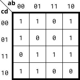
Kmap1
- Implement the circuit described by the Karnaugh map below.
module top_module(
    input a,
    input b,
    input c,
    output out  );

    assign out = a | b | c;

endmodule
Kmap2
- Implement the circuit described by the Karnaugh map below.
module top_module(
    input a,
    input b,
    input c,
    input d,
    output out  );

    // a'd' + b'c' + acd + a'bc
    wire w1, w2, w3, w4;

    assign w1 = (~a)&(~d);
    assign w2 = (~b)&(~c);
    assign w3 = a&c&d;
    assign w4 = (~a)&b&c;

    assign out = w1|w2|w3|w4;
endmodule
Kmap3
- Implement the circuit described by the Karnaugh map below.
module top_module(
    input a,
    input b,
    input c,
    input d,
    output out  );

    // a + b'c
    assign out = a | (~b&c);

endmodule
Kmap4
- Implement the circuit described by the Karnaugh map below.
module top_module(
    input a,
    input b,
    input c,
    input d,
    output out  );

    always @(*) begin
        if (a == b && c != d)
            out = 1;
        else if (a != b && c == d)
            out = 1;
        else
            out = 0;
    end

endmodule
Minimum SOP and POS
- A single-output digital system with four inputs (a,b,c,d) generates a logic-1 when 2, 7, or 15 appears on the inputs, and a logic-0 when 0, 1, 4, 5, 6, 9, 10, 13, or 14 appears. The input conditions for the numbers 3, 8, 11, and 12 never occur in this system. For example, 7 corresponds to a,b,c,d being set to 0,1,1,1, respectively.
- Determine the output out_sop in minimum SOP form, and the output out_pos in minimum POS form.
module top_module (
    input a,
    input b,
    input c,
    input d,
    output out_sop,
    output out_pos
);

    // f = d3 + m7 + d11 + m15 + m2
    // f = cd + a'b'c
    assign out_sop = (c & d) | (~a & ~b & c);
    // f' = m0 + m1 + m4 + m5 + m6 + d8 + m9 + m10 + d11 + d12 + m13 + m14
    // f' = c' + ab' + bd'
    // f = (c)(a'+b)(b'+d)
    assign out_pos = c & (~a | b) & (~b | d);

endmodule
Karnaugh map
- Consider the function f shown in the Karnaugh map below.
- Implement this function. d is don’t-care, which means you may choose to output whatever value is convenient.
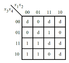
module top_module (
    input [4:1] x,
    output f );

    // x[2]x[4] + x[1]'x[3]
    assign f = (x[2] & x[4]) | (~x[1] & x[3]);

endmodule
Karnaugh map
- Consider the function f shown in the Karnaugh map below. Implement this function.
(The original exam question asked for simplified SOP and POS forms of the function.)

module top_module (
    input [4:1] x,
    output f
);

    // x[2]'x[4]' + x[1]'x[3] + x[2]x[3]x[4]
    assign f = (~x[2] & ~x[4]) | (~x[1] & x[3]) | (x[2] & x[3] & x[4]);

endmodule
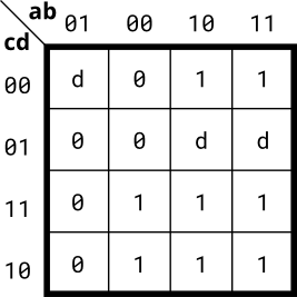
K-map implemented with a multiplexer
- For the following Karnaugh map, give the circuit implementation using one 4-to-1 multiplexer and as many 2-to-1 multiplexers as required, but using as few as possible. You are not allowed to use any other logic gate and you must use a and b as the multiplexer selector inputs, as shown on the 4-to-1 multiplexer below.
- You are implementing just the portion labelled top_module, such that the entire circuit (including the 4-to-1 mux) implements the K-map.
- (The requirement to use only 2-to-1 multiplexers exists because the original exam question also wanted to test logic function simplification using K-maps and how to synthesize logic functions using only multiplexers. If you wish to treat this as purely a Verilog exercise, you may ignore this constraint and write the module any way you wish.)
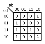
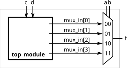
module top_module (
    input c,
    input d,
    output [3:0] mux_in
);
    assign mux_in[0] = c|d;  // 0111
    assign mux_in[1] = 1'b0; // 0000
    assign mux_in[2] = ~d;   // 1001
    assign mux_in[3] = c&d;  // 0010

endmodule
3.2 Sequential Logic
3.2.1 Latches and Flip-Flops
D flip-flop
- A D flip-flop is a circuit that stores a bit and is updated periodically, at the (usually) positive edge of a clock signal. D flip-flops are created by the logic synthesizer when a clocked always block is used (See alwaysblock2). A D + flip-flop is the simplest form of “blob of combinational logic followed by a flip-flop” where the combinational logic portion is just a wire.
- Create a single D flip-flop.
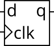
module top_module (
    input clk,    // Clocks are used in sequential circuits
    input d,
    output reg q );

    always @(posedge clk) begin
        q <= d;
    end

endmodule
D flip-flops
- Create 8 D flip-flops. All DFFs should be triggered by the positive edge of
clk.
module top_module (
    input clk,
    input [7:0] d,
    output [7:0] q
);

    always @(posedge clk) begin
        q <= d;
    end

endmodule
DFF with reset
- Create 8 D flip-flops with active high synchronous reset. All DFFs should be triggered by the positive edge of
clk.
module top_module (
    input clk,
    input reset,            // Synchronous reset
    input [7:0] d,
    output [7:0] q
);

    always @(posedge clk) begin
        if (reset) begin
            q <= 8'b0;
        end
        else begin
            q <= d;
        end
    end

endmodule
DFF with reset value
- Create 8 D flip-flops with active high synchronous reset. The flip-flops must be reset to 0x34 rather than zero. All DFFs should be triggered by the negative edge of
clk.
module top_module (
    input clk,
    input reset,
    input [7:0] d,
    output [7:0] q
);

    always @(negedge clk) begin
        if (reset) begin
            q <= 8'h34;
        end
        else begin
            q <= d;
        end
    end

endmodule
DFF with asynchronous reset
- Create 8 D flip-flops with active high asynchronous reset. All DFFs should be triggered by the positive edge of
clk.
module top_module (
    input clk,
    input areset,   // active high asynchronous reset
    input [7:0] d,
    output [7:0] q
);

    always @(posedge clk or posedge areset)
        if (areset)
            q <= 0;
        else
            q <= d;

endmodule
- In Verilog, the sensity list looks strange. The FF’s reset is sensitive to the level of areset, so why does using “posedge areset” work? To see why it works, consider the truth table for all events that change the input signals, assuming clk and areset do not swith at precisely the same time.
\(\begin{array}{|c|c|c|l|}\hline \text{clk}&\text{areset}&\text{output}&\text{comment}\\\hline \text{x}&\text{0}\rightarrow\text{1}&\text{q}\leftarrow{0;}&\text{because areset = 1}\\\hline \text{x}&\text{1}\rightarrow\text{0}&\text{no change}&\text{always block not triggered}\\\hline \text{0}\rightarrow\text{1}&\text{0}&\text{q}\leftarrow{d;}&\text{not resetting}\\\hline \text{0}\rightarrow\text{1}&\text{1}&\text{q}\leftarrow{0;}&\text{still resetting, q was 0 before too}\\\hline \text{1}\rightarrow\text{0}&\text{x}&\text{no change}&\text{always block not triggered}\\\hline \end{array}\)
DFF with byte enable
- Create 16 D flip-flops. It’s sometimes useful to only modify parts of a group of flip-flops. The byte-enable inputs control whether each byte of the 16 registers should be written to on that cycle.
byteena[1]controls the upper byted[15:8], whilebyteena[0]controls the lower byted[7:0].resetnis a synchronous, active-low reset. All DFFs should be triggered by the positive edge ofclk.
module top_module (
    input clk,
    input resetn,
    input [1:0] byteena,
    input [15:0] d,
    output [15:0] q
);

    always @(posedge clk) begin
        if (resetn == 1'b0) begin
            q <= 16'd0;
        end
        else begin
            case(byteena)
                0: q <= q;
                1: q <= {q[15:8], d[7:0]};
                2: q <= {d[15:8], q[7:0]};
                3: q <= d;
            endcase
        end
    end

endmodule
D Latch
- Implement the following circuit:
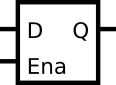
- Note that this is a latch, so a Quartus warning about hvaing inferred a latch is expected.
- 對於組合邏輯,if 若沒有補全 else,case 條件不完全,可能會產生 latch。但是如果中間的信號有初值,就不會產生 latch。所以要盡量避免 latch 的產生,避免對時序的危害很大。
module top_module (
    input d,
    input ena,
    output q);

    always @(*) begin
        if (ena == 1'b1)
            q = d;
    end

endmodule
DFFAR
- Implement the following circuit:
module top_module (
    input clk,
    input d,
    input ar,   // asynchronous reset
    output q);

    always@(posedge clk or posedge ar) begin
        if (ar == 1)
            q <= 0;
        else
            q <= d;
    end

endmodule
DFFR
- Implement the following circuit:
module top_module (
    input clk,
    input d,
    input r,   // synchronous reset
    output q);

    always@(posedge clk) begin
        if (r == 1) begin
            q <= 0;
        end
        else begin
            q <= d;
        end
    end

endmodule
DFF+gate
- Implement the following circuit:
module top_module (
    input clk,
    input in,
    output reg out);

    always@(posedge clk) begin
        out <= out ^ in;
    end

endmodule
- 注意
output需為reg型別。
Mux and DFF
- Consider the sequential circuit below:

- Assume that you want to implement hierarchical Verilog code for this circuit, using three instantiations of a submodule that has a flip-flop and multiplexer in it. Write a Verilog module (containing one flip-flop and multiplexer) named top_module for this submodule.
module top_module (
	  input clk,
	  input L,
    input r_in,
	  input q_in,
	  output reg Q);

    always@(posedge clk) begin
        if (L)
            Q <= r_in;
        else
            Q <= q_in;
    end

endmodule